When designing electronic devices it is often necessary to form pulses of a given length or to generate a rectangular signal with a given frequency and a certain length-to-pause ratio. An experienced designer can easily design such a device on separate digital elements, but it is more convenient to use a specialized chip for this purpose.
Contents
What is the NE555 and where it can be used
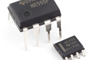
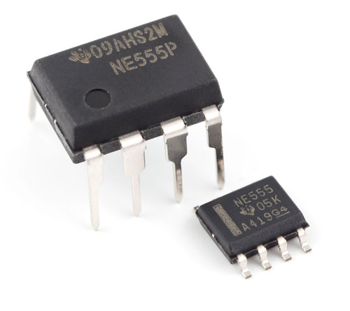
The NE555 was designed in the 1970s and is still very popular among professionals and amateurs. It is a timer encapsulated with 8 pins. It is available in DIP version or in different SMD versions.
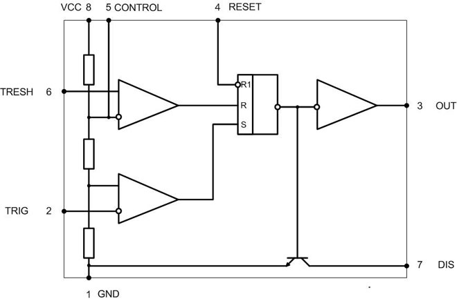
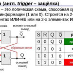
The microcircuit contains two comparators - upper and lower. On their inputs the reference voltage is formed, equal to 2/3 and 1/3 of the supply voltage. The divider is formed by resistors 5 kΩ resistors. The comparators control the RS trigger. A buffer amplifier and a transistor switch are connected to its output. Each comparator has one free input and is used to supply external control signals. The upper comparator triggers when a high level appears and turns the output of the chip to a low level. The lower one "monitors" the reduction of voltage below 1/3 VCC and sets the timer output to logical 1.
The main characteristics of the chip NE555
Timer characteristics of different manufacturers may differ within a small range, but in principle there are no deviations (except for chips of unknown origin, from them you can expect anything):
- The supply voltage is specified as +5V to +15V as standard, although datasheets have a range of 4.5...18V.
- The output current is 200 mA.
- The output voltage is maximum VCC minus 1.6 V, but not less than 2 V at 5 V supply voltage.
- Current consumption at 5 V is not more than 5 mA, at 15 V - up to 13 mA.
- Accuracy of pulse duration formation - not more than 2.25%.
- Maximum operating frequency is 500 kHz.
All parameters are given for ambient temperature +25 °С.
Pin assignment and arrangement
Timer pins are located in a standard way regardless of the case design - in ascending order from the key counterclockwise (when viewed from above), from 1 to 8. Each pin has a different function:
- GND - is the common wire of the device power supply.
- TRIG - When a low level is applied, it triggers the second (lower in the diagram) comparator, its output is a logical 1, which sets the internal RS-trigger to 0. It is connected to an external RC-chain timing circuit. It has priority over THR.
- OUT - output. High signal level just below the supply voltage, low signal level - 0,25 V.
- RESET - reset. Independent of signals on other inputs, if low, resets output to 0 and inhibits timer operation.
- CTRL - control. It always has a 2/3 voltage level on the power bus. An external signal can be applied here and the output can be modulated with it.
- THR - When a high level is reached (over 2/3 of the supply), the first (circuit top) trigger is set to 1 and the internal RS trigger The internal RS-trigger will go to 1.
- DIS - Discharge of the time capacitor. When the trigger output is high, the internal transistor opens and a fast discharge occurs. The timer is ready for the next duty cycle.
- VCC - Power supply output. It can be supplied with voltages from 5 to 15 V.
Description of the NE555 modes of operation
Although the architecture of the timer allows it to be used in different modes, there are three typical modes of operation of the NE555.
Single Vibrator (Standby Multivibrator)
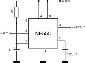
Initial position:
- At input 2, the logic level is high;
- On inputs R and S of the trigger - zeros;
- Trigger output - 1;
- discharge circuit transistor is open, capacitor C is bypassed;
- at output 3 - level 0.
When zero level appears on input 2, the lower comparator switches to 1, resetting the trigger to 0. A high level appears on the chip output. At the same time the transistor closes and stops shunting the capacitor. It starts charging through resistor R. As soon as the voltage on it reaches 2/3 of VCC the upper comparator goes off, sets the trigger back to 1 and the timer output to 0. The transistor opens and discharges the capacitor. This generates a positive pulse at the output, the beginning of which is determined by the external signal at input 2, and its end depends on the time of the capacitor charge, which is calculated by the formula t=1,1⋅R⋅C.
Multivibrator
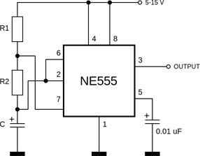
When the power supply is applied the capacitor is discharged, input 2 (and 6) is logic 0, the timer output is 1 (this process is described in the previous section). After charging the capacitor through R1 and R2 to 2/3 VCC the high level at input 6 will reset output 3 to zero and the discharge transistor will open. But the capacitor will not be discharged directly, but through R2. Eventually the circuit will return to its original position and the cycle will repeat over and over again. From the description of the process you can see that the charge time is determined by the sum of the resistances R1, R2 and the capacitor's capacity, and the discharge time is set by R1 and C. Instead of R1 and R2 you can put variable resistors and operatively control the frequency and pulse rate. Formulas for calculation:
- pulse duration t1=0.693⋅(R1+R2)⋅C;
- pause duration t2=0.693⋅R2⋅C;
- pulse repetition rate f=1/(0.693(R1+2⋅R2)⋅C.
The pause time cannot exceed the pulse time. To get around this limitation, discharge and charge circuits are separated by including a diode (cathode to pin 6, anode to pin 7).
Schmitt trigger
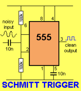
You can build a Schmitt trigger on a 555 chip. This device converts a slowly changing signal (sine, sawtooth, etc.) to a square wave. No timing circuits are used here, the signal is applied to inputs 2 and 6 connected to each other. When the 2/3 VCC threshold is reached, the output voltage jumps to 1, when it drops to 1/3 it also jumps down to zero. The zone of ambiguity is 1/3 of the supply voltage.
Advantages and disadvantages
The main advantage of the NE555 chip is its simplicity of use - to build a circuit it is enough to have a small, well-calculated package. At the same time, the cost of the device is low.
The main disadvantage of the timer is a pronounced dependence of the pulse duration on the supply voltage. This is due to the fact that the capacitor in a flicker or flicker circuit is charged through a resistor (or two), and the upper lead of the resistor is connected to the power bus. The current through the resistor is formed by the VCC voltage - the higher it is, the higher the current, the faster the capacitor will charge, the earlier the comparator will trigger, the shorter the generated time interval will be. For some unknown reason, this point is missing in the technical documentation, but it is well known to the developers.
Another disadvantage of the timer is that the threshold voltages of comparators are formed by internal dividers and cannot be adjusted. This narrows the application possibilities of the NE555.
And one more unpleasant feature. Due to the push-pull design of the output stage, at the moment of switching (when the upstream transistor is open and the downstream one is not yet closed or vice versa)) there is a through current pulse. Its duration is not long, but it leads to additional heating of the microcircuit and creates noise in the power circuit.
What are the analogues
Since the existence of the timer, developed and released a large number of clones. They are produced by different firms, but all contain in the name of the numbers 555. Among the factories that produce analogs, there are both popular manufacturers of electronic components, and unknown manufacturers from Southeast Asia. If the first ones provide the declared parameters, then you should not expect any guarantees from the second ones. Deviations from the declared characteristics can be large.
The USSR developed a similar timer, KR1006VI1. Its functionality is identical to the original with one exception: pin 2 has priority over pin 6 (and not the other way around as with the NE555). This should be taken into account when designing circuits. One more thing: the index KR means that the chip is only available in a DIP8 package.
Examples of Practical Application
The field of practical application of the timer is wide, within the limits of this review we can not fully disclose the topic. But the most common examples are worth parsing.
In single-oscillator mode on a few chips you can build a code lock with a time-limited dialing code. Another way is to use as a threshold indicator (light, capacity filling level, etc.) together with various sensors.
In the multivibrator mode (astable mode) the timer finds the widest application. On several timers you can build a daisy chain switch with separate control of the flashing frequency, ON time and pause time. You can use the NE555 as the basis for a time relay and form a time for switching on consumers from 1 to 25 seconds. You can build a metronome for a musician. This is the most used mode of the chip and it is impossible to describe all the uses.
As a Schmitt trigger the timer is not often used. But in bistable mode without frequency drivers the NE555 is used as a contact bounce suppressor or a two-button switch in start-stop mode. In fact, only the built-in RS trigger is used. It is also known about building on the basis of a timer PWM regulator.
There are collections of circuits that describe various uses of the NE555 timer. They describe thousands of ways to use the chip. But the inquisitive mind of the designer may not be enough, and he will find an additional, not yet described anywhere else use of the timer. The possibilities laid down by the designers of the chip allow this.
Related articles: