The use of semiconductor devices (SSD) is widespread in radio electronics. This has reduced the size of various devices. The bipolar transistor is widely used, due to some features its functionality is wider than that of a simple field-effect transistor. To understand what it is used for and under what conditions it is used, it is necessary to consider its principle of operation, connection methods and classification.
Contents
Design and Operation Principle
The transistor is an electronic semiconductor which consists of 3 electrodes, one of which is the controlling one. Bipolar transistor differs from polar transistor in the presence of two types of charge carriers (negative and positive).
Negative charges represent electrons that are released from the outer shell of the crystal lattice. The positive type of charge, or holes, are formed in place of the released electron.
The design of a bipolar transistor (BT) is quite simple, despite its versatility. It consists of 3 conductor-type layers: an emitter (E), a base (B) and a collector (C).
Emitter (from Latin "to release") is a type of semiconductor junction whose main function is to inject charges into the base. The collector (Latin for "collector") serves to receive the emitter charges. The base is the control electrode.
The emitter and collector layers are almost identical, but differ in the degree to which impurities are added to improve the characteristics of the sensor. Adding impurities is called doping. For the collector layer (CL), the doping is weakly expressed to increase the collector voltage (Uk). The emitter semiconductor layer is heavily doped in order to increase the reverse allowable U of breakdown and improve carrier injection into the base layer (increases the current transfer coefficient - Kt). The base layer is doped weakly to provide more resistance (R).
The transition between base and emitter is smaller in area than K-B. The difference in area is what improves the Kt. The K-B junction is switched on with a reverse bias to release most of the heat Q, which is dissipated and provides better cooling of the crystal.
The performance of the BT depends on the thickness of the base layer (BS). This dependence is a value that varies by an inversely proportional relationship. A smaller thickness results in faster performance. This dependence is related to the transit time of the charge carriers. However, at the same time, Uk decreases.
A strong current flows between the emitter and K, called K current (Ik). Between E and B flows a small current, called B current (Ib), which is used for control. When Ib changes, there will be a change in Ik.
The transistor has two p-n junctions: E-B and K-B. When active, E-B is connected with forward bias, and K-B is connected with reverse bias. Since the E-B junction is open, the negative charges (electrons) flow into B. After that their partial recombination with holes takes place. However, most of the electrons reach K-B because of the small doping and thickness of B.
In BS, the electrons are nonessential charge carriers, and the electromagnetic field helps them to overcome the K-B transition. As Ib increases, the E-B opening will widen and more electrons will run between E and K. In this case there will be a significant amplification of the low-amplitude signal, because Ik is greater than Ib.
In order to understand the physical meaning of the bipolar type transistor more easily, it is necessary to associate it with a clear example. We have to assume that the pump to pump water is the power source, the water tap is the transistor, the water is Ik, the degree of turn of the tap knob is Ib. To increase the head you need to turn the tap a little - to perform a control action. Based on the example, we can conclude about the simple principle of PP operation.
However, with a significant increase in U at the K-B junction a shock ionization can occur, the consequence of which is an avalanche multiplication of the charge. When combined with the tunnel effect, this process gives an electrical and, with increasing time, a thermal breakdown, which puts the BC out of action. Sometimes the thermal breakdown occurs without the electrical breakdown as a result of a significant increase in current through the collector output.
In addition, when U changes on K-B and E-B, the thickness of these layers changes, if B is thin, there is a bowing effect (it is also called B puncture), in which the K-B and E-B junctions are connected. As a result of this phenomenon, the PP ceases to perform its functions.
Modes of Operation
A bipolar type transistor can operate in 4 modes:
- Active.
- Cutoff (RO).
- Saturation (SS).
- Barrier (RB).
Active mode of BTs can be normal (NAR) and inverse (IAR).
Normal active mode
In this mode, U, which is direct and is called E-B voltage (Ue-B), flows at the E-B junction. The mode is considered optimal and is used in most circuits. The E junction injects charges into the base region, which move to the collector. The latter accelerates the charges, creating a gain effect.
Inverse Active Mode
In this mode the K-B junction is open. The BT operates in the opposite direction, i.e., from K there is injection of hole charge carriers passing through B. They are collected by the E transition. The gain properties of the BT are weak, and BTs are rarely used in this mode.
Saturation mode.
In PH, both junctions are open. When E-B and K-B are connected to external sources in the forward direction, the BT will operate in PH. The diffusion electromagnetic field of E and K junctions is attenuated by the electric field generated by external sources. As a result, there will be a decrease in the barrier capability and a limitation of the diffusion capability of the main charge carriers. Hole injection from E and K junctions to B begins. This mode is mostly used in analog technology, but in some cases there may be exceptions.
Cutoff Mode
In this mode, the BT is completely closed and unable to conduct current. However, there are insignificant fluxes of nonessential charge carriers in the BT, creating thermal currents with small values. This mode is used in various types of overload and short-circuit protection.
Barrier Mode
The base of a PD is connected through a resistor to a K. A resistor is included in the K or E circuit, which sets the amount of current (I) through the PD. The BR is often used in circuits because it allows the BTs to operate at any frequency and over a larger temperature range.
Wiring Diagrams
For correct application and wiring of PDs, you need to know their classification and type. Classification of Bipolar Transistors:
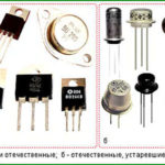
- Material of manufacture: germanium, silicon and arsenide gallium.
- Fabrication features.
- Power dissipation: low-power (up to 0.25 W), medium-power (0.25-1.6 W), high-power (above 1.6 W).
- Frequency limit: low-frequency (up to 2.7 MHz), medium-frequency (2.7-32 MHz), high-frequency (32-310 MHz), ultrahigh-frequency (over 310 MHz).
- Functional Purpose.
The functional purpose of BTs is divided into the following types:
- Low-frequency amplifiers with normalized and non-normalized noise figure (NNNKNSH).
- High-frequency amplifiers with NiNKNSH.
- Amplifying ultrahigh-frequency with NiNNFSH.
- Powerful high voltage amplifier.
- Generator with high and ultrahigh frequencies.
- Low-power and high-power high voltage switching.
- Pulsed high-power for high U-value operation.
In addition, there are these types of bipolar transistors:
- P-n-p.
- N-p-n.
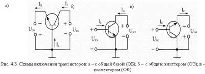
There are 3 circuits for switching a bipolar transistor, each with its own advantages and disadvantages:
- General B.
- Common E.
- Common K.
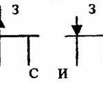
Common Base (CB) Switching
The circuit is used at high frequencies, allowing optimal use of the frequency response. Connecting one BT in Oh mode and then in an OB mode will amplify its frequency response. This connection scheme is used in antenna type amplifiers. The noise level at high frequencies is reduced.
Advantages:
- Optimal temperature values and wide frequency range (f).
- High Uk value.
Disadvantages:
- Low I gain.
- Low input R.
Open emitter (OhE) connection
With this circuit the U and I amplification occurs. The circuit can be powered from a single source. Often used in power amplifiers (P).
Advantages:
- High I, U, P gain.
- Single power supply.
- It inverts the output alternating U relative to the input.
It has significant disadvantages: the lowest temperature stability and frequency response is worse than for OB connection.
Common Collector Connection (OC)
The input U is fully transmitted back to the input, and the Ki is similar to the OC connection, but the U is low.
This type of inclusion is used for matching stages made on transistors, or with an input signal source that has a high output R (condenser-type microphone or sound pickup). The advantages are the high input R value and the low output R value. The disadvantage is the low U-amplification.
The main characteristics of bipolar transistors
Main characteristics of BTs:
- I gain.
- Input and output R.
- Inverse I-ke.
- Turn-on time.
- Frequency of transmission Ib.
- Inverse Ik.
- Maximum I-value.
Applications
Bipolar transistors are widely used in all fields of human activity. The main application is in devices for amplification, generation of electrical signals, as well as switching elements. They are used in various power amplifiers, in ordinary and switched-mode power supplies with the possibility of regulating U and I values, in computer technology.
In addition, they are often used to build various consumer protection against overloads, spikes in U, short circuits. Widely used in mining, metallurgical industries.
Related articles: